
Scanning Auger Electron Nanoprobe
Physical Electronics 710
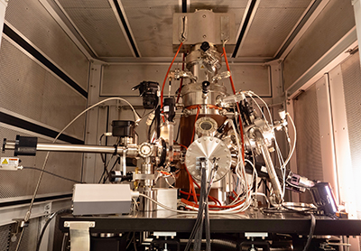
ICAL has recently acquired a Physical Electronics model 710 Scanning Auger NanoProbe, with EDS (Energy Dispersive X-ray Spectroscopy) and EBSD (Electron Backscattered Diffraction) capabilities. In Auger spectroscopy (AES), like SEM, a highly focused and energetically well-defined electron beam is incident on the sample. Electrons ejected from the sample are analyzed in terms of their kinetic energy and quantity. Some of these electrons are characteristic Auger electrons and much like the x-rays, the Auger electrons are the fingerprint of the atoms from which they are emitted.
Because of the low kinetic energies of the ejected Auger electrons, their escape depth is limited to a few atomic layers such that one can analyze only the top atomic layers of the sample of interest. Therefore, Auger is a surface-sensitive technique (~5nm) which complements the bulk x-ray microanalysis (~3um) of EDS. To look below the surface of the sample, the system is equipped with an in situ Ar-ion etching capability for depth profiling of the sample and charge compensation for insulating samples. The system operates under ultrahigh vacuum conditions with rapid sample introduction facilities. A secondary electron detector on this system allows high resolution imaging as previously described. With the exception of H and He, all elements can be detected.
In summary , the advantages of Auger electron spectroscopy are:
- Low-Z elemental detection
- Quantitative analysis, mapping, linescan for AES and EDS
- Surface sensitivity of 1-5 nm
- Enhanced lateral spatial resolution for elemental analysis (<8nm with a 20kV, 1nA electron beam)
- Limited chemical information
- Sputter depth profiling (three dimensional analysis)
- High resolution secondary electron imaging of anlysis area